-
Leon Zhang sales consultant
-
Email: zxl635973785@gmail.com
-
Phone/WhatsApp: +86 13655813266


Transformer High Backup Protection Relay
The Transformer High Backup Protection Relay is designed for backup protection of transformers in substations at voltage levels of 110 kV and below. It works in conjunction with the AST-441H Differential Protection Unit to perform secondary functions for the main transformer bay.
Product Functions (ANSI)
51V, 51N, 49, 27, 81U, 81O, 51I, 46, 59
Communication Mode
- Optional: RS-485, CAN bus, Ethernet, IEC 60870-5-103 (IEC-103)
In-house Factory & Technical Team, OEM ODM Custom Electrical Equipment
Send your requirements, we will quote for you within 12 hours
Description
Product Overview
- The Transformer High Backup Protection Relay is designed for backup protection of transformers in substations at voltage levels of 110 kV and below. It works in conjunction with the AST-441H Differential Protection Unit to perform secondary functions for the main transformer bay.
Product Functions (ANSI)
- Voltage-Dependent Overcurrent Protection|51V
- Residual Current Protection|51N
- Thermal Overload Protection|49
- Undervoltage Protection|27
- Underfrequency Protection|81U
- Overfrequency Protection|81O
- Inverse Overcurrent Protection|51I
- Current Unbalance Protection|46
- Overvoltage Protection|59
- VT (Voltage Transformer)
Communication Mode
- Optional: RS-485, CAN bus, Ethernet, IEC 60870-5-103 (IEC-103)
Main Functional Specifications
| No. | Parameter Category | Parameter Name | Technical Specification |
|---|---|---|---|
| 1 | Protection Response Characteristics | Protection Response Time (including output relay response time) | Average error in response time: ≤ 35 ms |
| 2 | Operating Range & Setting Accuracy | Precision Operating Range – Current | Minimum precision current: 0.08 In; Maximum precision current: 20 In |
| 3 | Operating Range & Setting Accuracy | Current Setting Error | When current exceeds 1.00 A, error shall not exceed ±2.5% |
| 4 | Operating Range & Setting Accuracy | Voltage Setting Error | Error shall not exceed ±3% |
| 5 | Measurement Accuracy | Current (I) / Voltage (U) Measurement Accuracy | Class 0.2 |
| 6 | Measurement Accuracy | Active Power (P) / Reactive Power (Q) Measurement Accuracy | Class 0.5 |
| 7 | Other Performance Indicators | Remote Signal (SOE) Resolution | ≤ 2 ms |
Event Logging, Fault Recording
- Recorded events consist of protection actions and device faults.
-
It records trip type, trip time and on-site operating parameters during tripping.
-
Fault records include protection operation time, operation type and RMS values pre and post recording.
-
Fault waveform: 2 cycles before fault, 4 cycles after fault.
-
Up to 48 SOE records and 16 fault reports can be retained after power outage.
Monitoring Features
- The Transformer High Backup Protection Relay measures analog parameters including current, voltage and frequency.
- It acquires status signals from circuit breakers, energy storage units, disconnectors and remote/local switches, along with other digital inputs. It also supports disconnector control functions.
Setting Table of Transformer High Backup Protection Relay
| No. | Parameter Name | Setting Range | Step Multiplier |
|---|---|---|---|
| 5 | Stage 1 Overcurrent Protection Time Delay (T1) | 0~120.00 s | ×100 |
| 6 | Stage 2 Overcurrent Protection Time Delay (T2) | 0~120.00 s | ×100 |
| 7 | Stage 3 Overcurrent Protection Time Delay (T3) | 0~120.00 s | ×100 |
| 8 | Spare | – | – |
| 9 | Stage 1 Zero-sequence Overcurrent Protection Time Delay (T01) | 0~120.00 s | ×100 |
| 10 | Stage 2 Zero-sequence Overcurrent Protection Time Delay (T02) | 0~120.00 s | ×100 |
| 11 | Zero-sequence Overvoltage Protection Time Delay (T0V) | 0~120.00 s | ×100 |
| 12 | Overload Protection Time Delay (TOL) | 0~120.00 s | ×100 |
| 13 | Undervoltage Protection Time Delay (TUV) | 0~120.00 s | ×100 |
| 14 | Under-frequency / Phase Loss Protection Time Delay (TUF/PL) | 0~120.00 s | ×100 |
| 15 | Stage 1 Overcurrent Protection Setting (Instantaneous Trip Current Setting) | 0.40~99.99 A / 0.10~20.00 A | ×100 |
| 16 | Stage 2 Overcurrent Protection Setting (Time-limited Instantaneous Trip Current Setting) | 0.40~99.99 A / 0.10~20.00 A | ×100 |
| 17 | Stage 3 Overcurrent Protection Setting (Overcurrent Protection Current Setting) | 0.40~99.99 A / 0.10~20.00 A | ×10 |
| 18 | Overload Protection Setting (Overload Current Setting) | 0.40~99.99 A / 0.10~20.00 A | ×100 |
| 19 | Stage 1 Inverse-time Overcurrent Protection Current Setting (Original Start-up Setting) | 1~99.99 A | ×100 |
| 20 | Stage 1 Zero-sequence Overcurrent Protection Setting | 0.02~5.00 A / 0.40~99.99 A | ×100 |
| 21 | Stage 2 Zero-sequence Overcurrent Protection Setting | 0.02~5.00 A / 0.40~99.99 A | ×100 |
| 22 | Zero-sequence Current Blocking Setting (Zero-sequence Current for Zero-sequence Overvoltage Blocking) | 0.02~5.00 A / 0.40~99.99 A | ×100 |
| 23 | Undervoltage Blocking Setting (Undervoltage for Overcurrent Protection Blocking) | 5~100.00 V | ×100 |
| 24 | Negative-sequence Voltage Setting (Negative-sequence Voltage for Overcurrent Protection Blocking) | 5~100.00 V | ×100 |
| 25 | Zero-sequence Overvoltage Protection Setting | 5~100.00 V | ×100 |
| 26 | Zero-sequence Voltage Blocking Setting (Zero-sequence Voltage for Zero-sequence Overcurrent Blocking) | 0~100.00 V | ×100 |
| 27 | Undervoltage Protection Setting (Undervoltage Trip Setting) | 0~100.00 V | ×100 |
| 28 | Under-frequency Protection Setting | 0.2~10.00 Hz | ×100 |
| 29 | Stage 1 Inverse-time Overcurrent Protection Time Delay | 0~120.00 s | ×100 |
| 30 | Current Unbalance Protection Time Delay | 0~120.00 s | ×100 |
| 31 | Current Blocking Setting (Low Current for Under-frequency Protection Blocking) | – | – |
| 32 | Voltage Blocking Setting (Low Voltage for Under-frequency Protection Blocking) | – | – |
| 33 | Frequency Slip Setting | – | – |
| 34 | Stage 2 Inverse-time Overcurrent Protection Time Constant | 0~120.00 s | ×100 |
| 35 | Stage 2 Inverse-time Overcurrent Protection Current Setting | 1~99.99 A | ×100 |
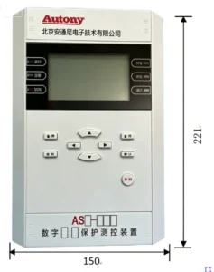
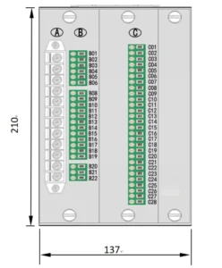
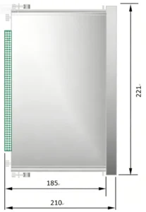
Outline and Installation Dimensions

FAQ
Q:What is transformer backup protection?
A:The primary scope of Transformer High Backup Protection Relay covers the areas outside the bushing. When a fault occurs externally, the transformer backup protection device operates; it also serves as the transformer’s secondary backup protection, activating when the main protection fails to operate.
Q:How to Install and Use a Transformer Backup Protection Device
A:When selecting backup protection devices for transformers, it is necessary to consider their protective functions and other technical parameters. Equipment such as transformer differential protection devices and non-electrical quantity protection devices should be installed together in a single control panel.
Q: What are the main protection functions?
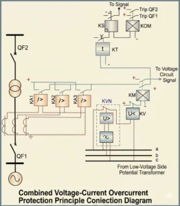
A: Voltage restrained phase overcurrent, zero-sequence earth overcurrent, overvoltage and undervoltage backup protection.
2 reviews for Transformer High Backup Protection Relay
Related products

")


High Quality
Stable performance, reliable design, ensuring safe operation for power system protection and grid stability.
Fast Delivery
Timely delivery to support your urgent orders and project schedules efficiently and professionally at any time.
Best Warranty
Professional Warranty: Reliable after-sales support for stable relay protection and long-term customer satisfaction.
xiao zhang –
The relay monitors HV side voltage and current in real time. For system short-circuit or grounding faults that primary differential protection fails to cut off, it operates with preset delay to trip the breaker. Voltage restraint avoids misoperation under normal overload conditions.
Jack –
Sensitive and selective coordination — avoids unnecessary outages.